|
|
|
|
|
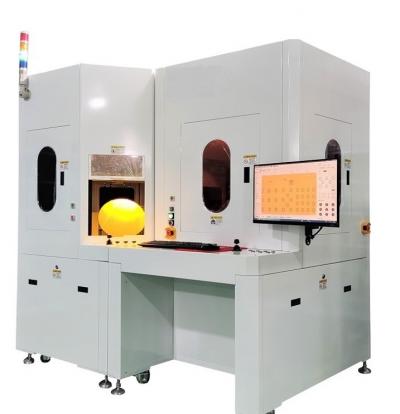
| We provide a macro inspection system for wafer surface defects after photolithography developed process, Etching, or CMP in wafer manufacturing. It can detect defects or water marks on the front or back of the wafer. There is also a C-clamp to turn the wafer over and then have an engineer or operator inspect the center area of the backside of the wafer for defects. After the macro inspection, the robot system transfers the wafer to the microscope for microscopic automatic detection. The microscope has five different magnification lenses to choose from.
1. Wafer surface front/back macro inspection.
2. Two different wafer back flipping methods.
3. Microscope five different magnification lens options, 5x, 10x, 20x, 50x, 100x.
4. Microscope with x-y automation stage.
5. High-standard German-made Basler industrial cameras and smart vision software can be added.
6. If there are metal frame rings, blue film tape, and custom-made 13-piece wafer cassettes in the wafer manufacturing process, we also have custom-made model.
|
|
|
|
| |
|